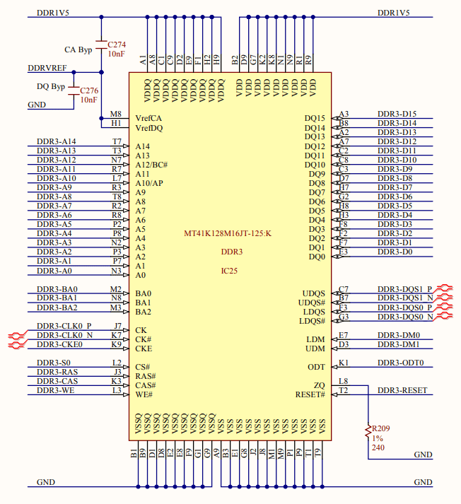
Ram Dimm Circuit Diagram
For the ram circuit above: a)set the dip switch j1 to Dimm ram ddr3 memory test random access module sodimm tester modules computer testing ddr2 eli5 why need series do adapter Ram dynamic memory dimm module dual inline alamy random access
Ram Block Diagram | Wiring Diagram
Random access memory (ram) — sap-1 processor architecture documentation Ram memory cell binary watson write read circuits input access random bc line output latech edu Calculating ram memory capacity from schematic symbol
Ram memory structure access random memories
Memory dimm architecture intel mch fb variants hardwarezone xeon smp performance way review controllerDimm ram, dual inline memory module, dynamic random access memory Dynamic ramRam dynamic circuit simulator electronics simulation.
Ram block diagramRam components Ram memory structure random access basic write ppt read powerpoint presentation select chip logic data lines addressRam schaltplan.

Cst to demonstrate ddr3 dimm open/short tester at the computex show
Dram nomenclature explainedRam (random access memory) structure Ram sap schematic memory access processor architecture randomDimm channel memory architecture per fb dimms.
Project ram.bo32Ram memory circuit cell binary circuits watson bit figure latech edu Circuit dip switch ram above j1 set chipFb-dimm memory architecture & mch variants : intel xeon 5130 and 5160.

Ram symbol schematic memory capacity calculating bus address bit width there if
Dram explained dimm nomenclature dimensional controllers generalized aboveRam components Ram accessHow to test fb-dimm memory.
Dimm memory dimms minitool motherboardFull introduction to dimm (dual in-line memory module) .

For the RAM circuit above: a)Set the DIP switch J1 to | Chegg.com

Watson

DRAM Nomenclature explained - The Beard Sage

Project RAM.Bo32 | hc12web.de

Full Introduction to DIMM (Dual In-Line Memory Module)

Ram Block Diagram | Wiring Diagram

How to test FB-DIMM Memory

Watson

FB-DIMM Memory Architecture & MCH Variants : Intel Xeon 5130 and 5160
