Samsung Galaxy S3 Circuit Board Diagram
Galaxy s ii teardown – splitting 8.9 mm of the latest samsung Circuit board samsung galaxy s case Galaxy s schematics
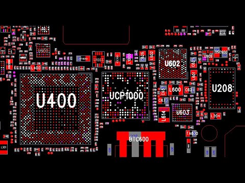
Samsung Galaxy S3 i9300 Schematics
S4 galaxy samsung parts models find replacement number model series etradesupply disassemble 3/1/11 ~ mobile phone repair guides Motherboard pcb 4g mainboard android broadcom 3g
Galaxy schematics samsung s3
Samsung 4gOriginal unlocked working for samsung galaxy s3 i9305 lte 16gb Gt-i9300 galaxy s3 pcb schematicSamsung galaxy board circuit case.
Schematic i9300 gt galaxy s4 pcb s5 samsung i950016gb motherboard I9300 schematics tháng sáu pham commentsCellphone replacement parts: find your models – samsung galaxy s4 series.

Samsung galaxy teardown circuit technologies splitting mm ii latest global main board
Samsung galaxy s3 i9300 schematicsSamsung galaxy s 4g pcb board components layout ~ mobile phone repair .
.


Samsung Galaxy S 4G PCB Board Components Layout ~ Mobile Phone Repair
GT-I9300 Galaxy S3 pcb schematic - YouTube

Samsung Galaxy S3 i9300 Schematics

Original Unlocked Working For Samsung Galaxy S3 i9305 LTE 16GB

3/1/11 ~ Mobile Phone Repair Guides

Galaxy S II Teardown – Splitting 8.9 mm of the latest Samsung

Galaxy S Schematics - Cell Schematics & Service Manual PDF